
At 1.6 Tbps per port, optical interconnect stops being a component problem and becomes a packaging problem. Two walls arrive at roughly the same time: the power burned by electrical SerDes, and the amount of heat you can physically get out of a faceplate. Neither is solved by making the optics faster, which is why the interesting engineering has moved to the seam between materials.
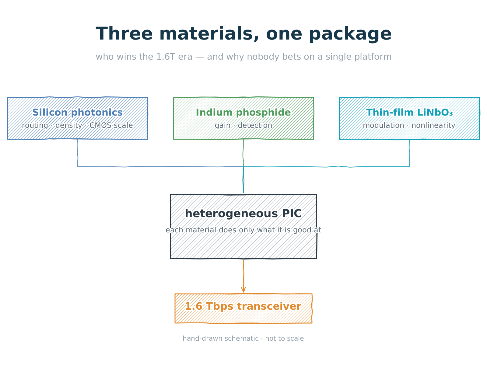
A packaging-first look at silicon photonics, indium phosphide and thin-film lithium niobate.
1. The two walls
The first wall is electrical. Pushing 200 Gbps per lane across a PCB means the SerDes — not the optics — takes the largest share of the link power budget. Every centimetre of trace between the switch ASIC and the optical engine has to be equalised, and equalisation costs energy that no optical improvement can recover.
The second wall is thermal and mechanical. Pluggable modules at the faceplate are already power-dense enough that airflow is the limiting factor, and the panel area available for cages does not grow with bandwidth. The obvious fix is to move the optics closer to the switch, but that trades a solved problem (serviceability, interoperability, a mature multi-vendor ecosystem) for a set of unsolved ones.
2. Three materials, three sets of physics
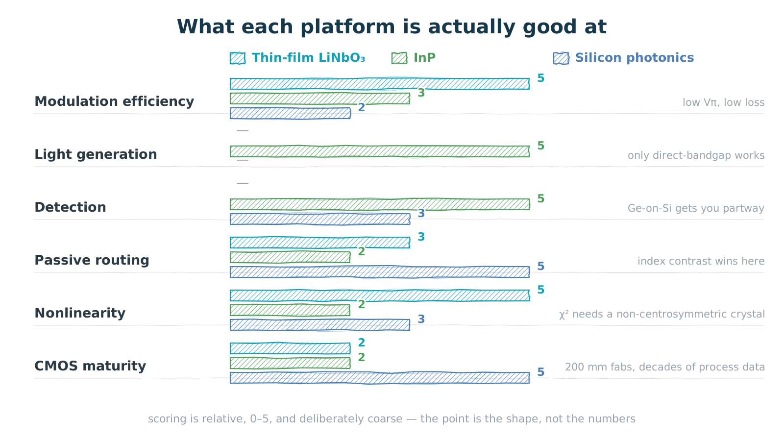
Figure 1|What each photonic platform is actually good at, scored 0–5 on six axes
the shape matters more than the numbers: no platform fills the grid
Silicon photonics wins on geometry and on manufacturing. The index contrast between silicon and silica is enormous, so bends can be a few microns and a whole transceiver's worth of routing fits on a die measured in millimetres. It runs in 200 mm fabs with decades of process data behind them. What it cannot do is generate light — silicon has an indirect bandgap — and its electro-optic effect is weak enough that practical modulators lean on free-carrier plasma dispersion, which introduces loss and drifts with temperature.
Indium phosphide is the opposite case. It is a direct-bandgap III-V, so lasers, semiconductor optical amplifiers and high-speed detectors all come naturally; waveguide photodetectors in this material system reach 3 dB bandwidths around 110 GHz with usable dark current. The constraints are economic and geometric: wafers are small, epitaxy is expensive, and the index contrast is modest enough that passive circuits are bulky by silicon standards.
Thin-film lithium niobate brings the strongest practical Pockels effect of the three, plus a usable second-order nonlinearity and very low waveguide loss. Bonding a sub-micron film onto silica raises the index contrast enough to pull the electrodes close, which collapses the voltage–length product and with it the driver power. But it generates nothing, detects nothing, and its volume-manufacturing base is the youngest of the three.
3. Why nobody wins alone
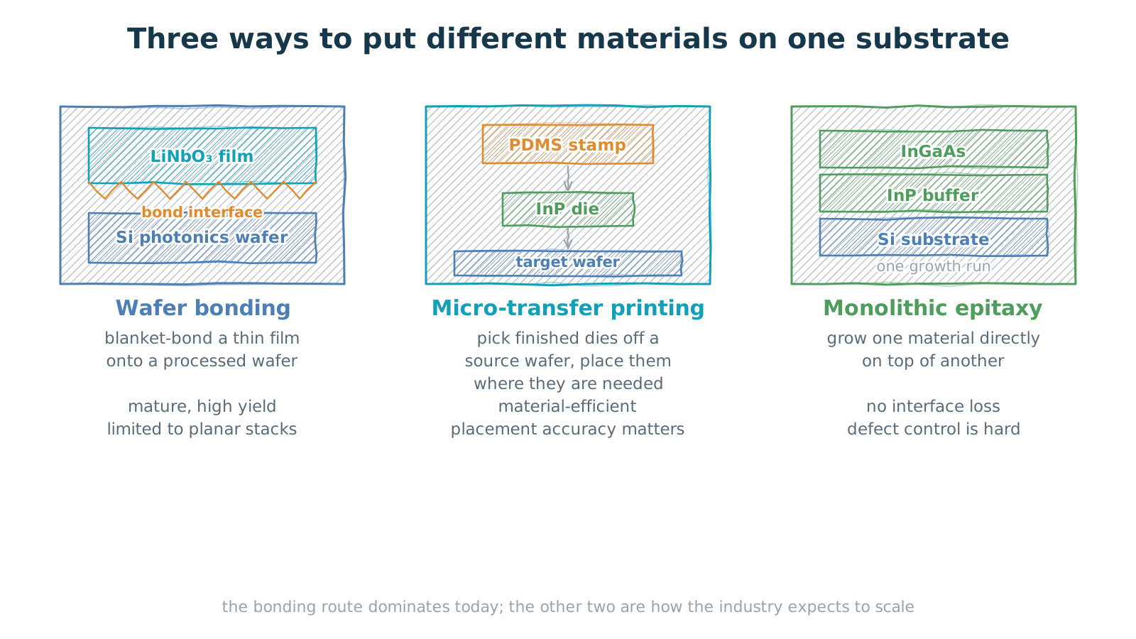
Figure 2|Three routes to putting different materials on one substrate
wafer bonding carries most of today's product; the other two are how the industry expects to scale
Read those three paragraphs together and the conclusion is uncomfortably clear: each platform is excellent at exactly one-third of a transceiver. The best modulator material cannot make a photon. The best light source makes expensive waveguides. The best routing platform cannot modulate efficiently.
So the competitive question is not which material wins — it is who can combine them at volume. Wafer bonding, where a thin film of one material is bonded blanket-style onto a processed wafer of another and then etched, is what most shipping products use today. It is mature and high-yield, but it is fundamentally a planar stack.
The two routes getting the most attention for what comes next are micro-transfer printing, which picks finished dies off a source wafer and places them only where they are needed, and monolithic epitaxy, growing one material directly on another. The first is material-efficient and allows real layout freedom; the second removes the coupling interface entirely, at the cost of defect control that is still hard.
4. Where the decibels actually go
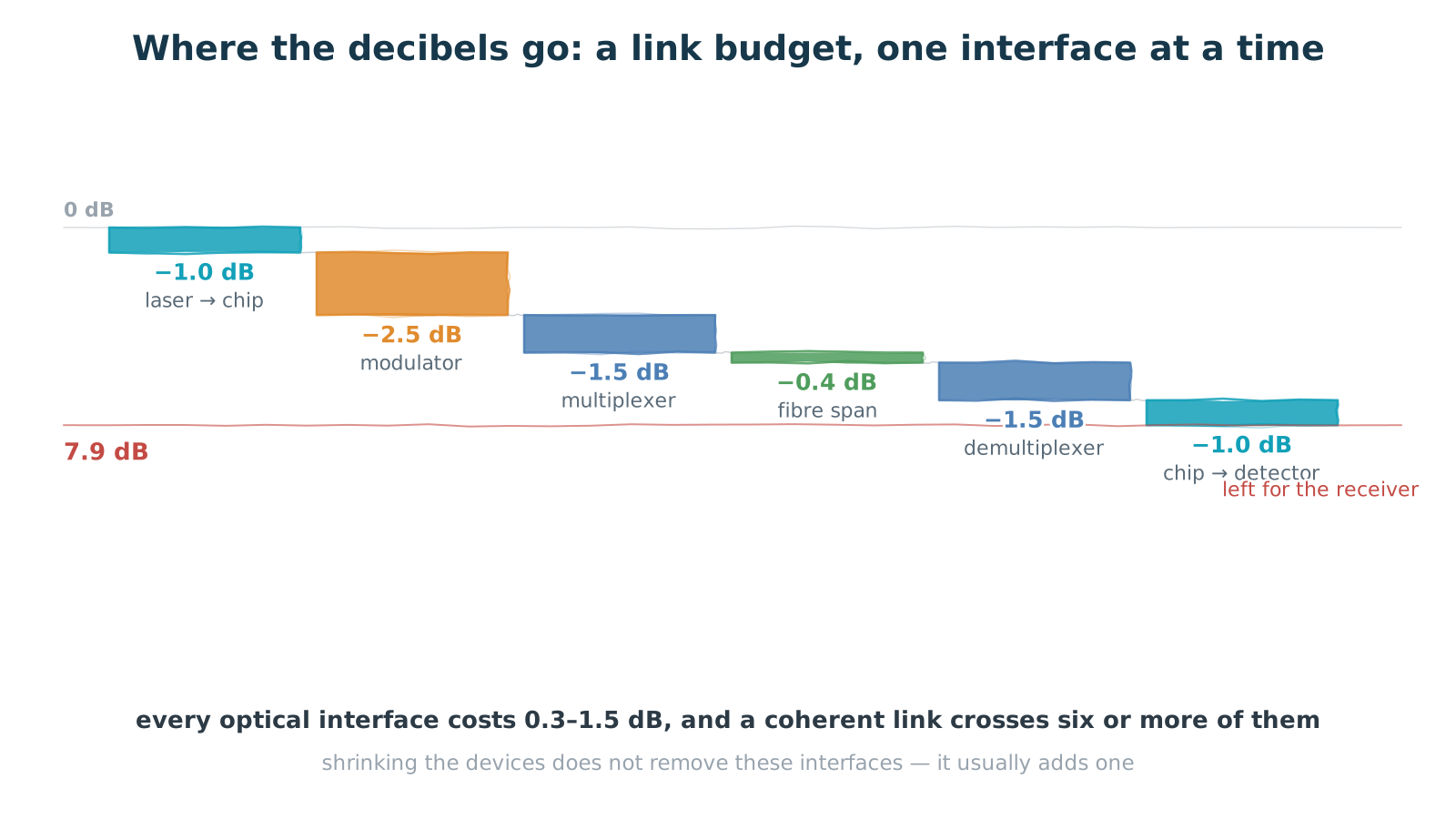
Figure 3|A coherent link's optical budget, lost one interface at a time
each interface costs 0.3–1.5 dB, and miniaturisation tends to add interfaces rather than remove them
There is a temptation to assume that shrinking devices also shrinks the loss. A link budget is a useful cure for it. Every optical interface — laser to chip, modulator in and out, multiplexer, fibre, demultiplexer, back into the detector — takes its own slice, typically somewhere between 0.3 and 1.5 dB. Six of them and you have given away a substantial fraction of the transmitter's output before the signal has travelled anywhere.
This is why the industry talks so much about coupling. A modulator with excellent loss per centimetre is worth much less if getting light into and out of it costs 2 dB per facet. It is also why co-design beats component selection: the interfaces are where the budget goes, and interfaces are a packaging decision, not a device one.
5. Shrinking the electrical reach
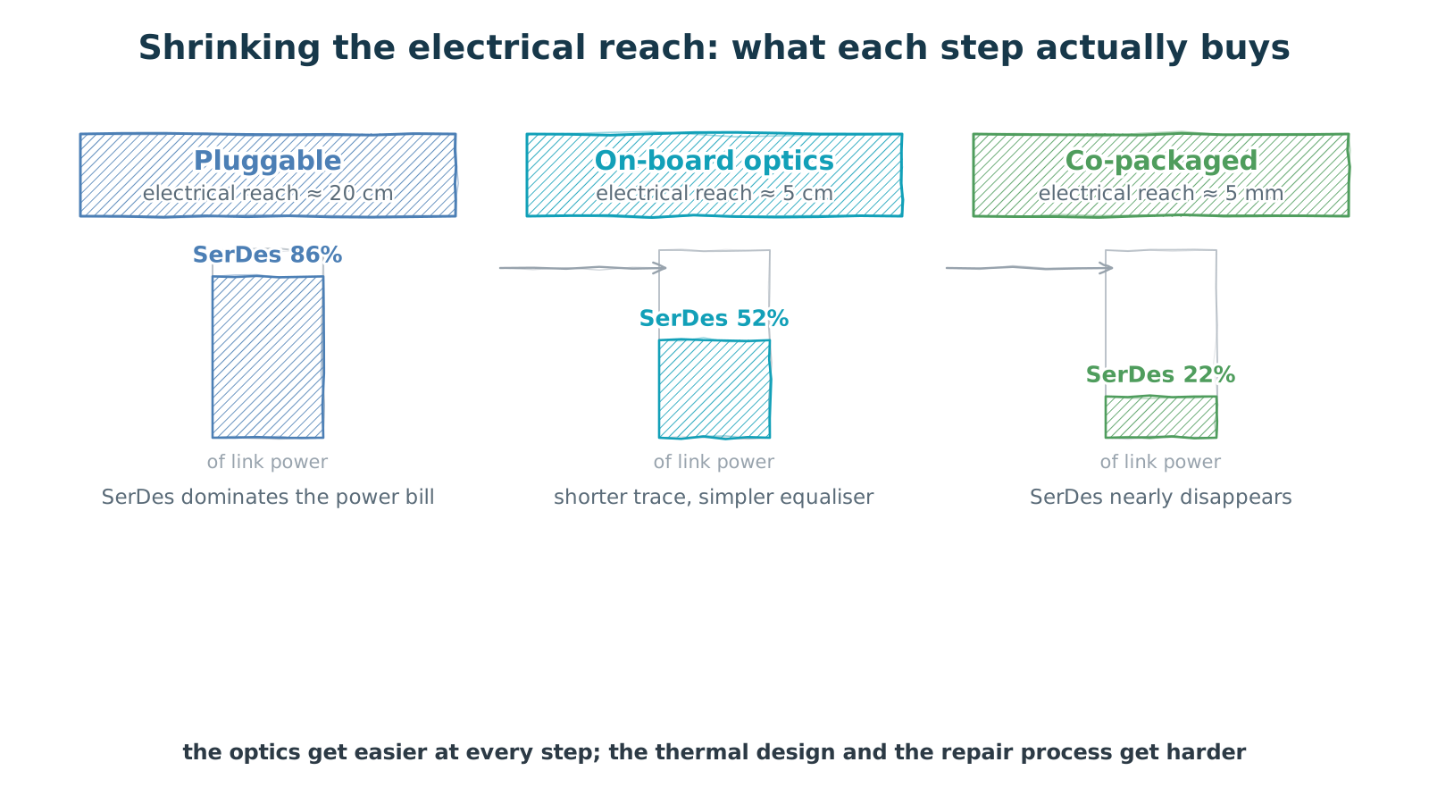
Figure 4|What each step toward the switch actually buys: SerDes power as a share of link power
the optics get easier at every step; thermal design and the repair process get harder
The cleanest way to see the packaging argument is to follow the electrical trace. In a faceplate pluggable it runs roughly 20 cm and the SerDes dominates the power bill. On an on-board optical engine the trace drops to a few centimetres and the equaliser gets simpler. In a co-packaged design the distance is millimetres and the SerDes almost disappears from the budget — that is where the large efficiency gains come from, not from any improvement in the optics themselves.
What gets harder at each step is everything around the optics. Fibre attach at high density has to remain serviceable. Optical dies need known-good-die testing at wafer level, because you cannot repair a co-packaged assembly by swapping a module. Thermal design has to keep temperature-sensitive optical devices stable next to a switch chip dissipating hundreds of watts. These are the problems that decide timing, and they are not device-physics problems.
6. Reading the cost curve
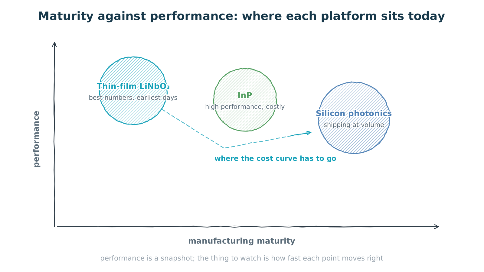
Figure 5|Maturity against performance: where each platform sits today
performance is a snapshot; the thing to watch is how fast each point moves to the right
Position the three platforms on maturity against performance and the picture is stable and slightly misleading. Silicon photonics sits far right and mid-height: shipping at volume, good enough for most short-reach work. Indium phosphide sits high and further left: excellent devices, real cost pressure. Thin-film lithium niobate sits highest and furthest left: the best numbers, the earliest days.
The snapshot understates what matters, which is velocity. For anyone making a platform decision, the useful questions are plainer than they sound. Can this device hold its datasheet numbers at full load, high temperature, over long operating hours? What is the coupling loss at every interface, and how is it tested in production? And at your volume, where does the cost curve sit next year rather than today? These decide architectures far more often than a headline specification does.
Closing: the moat is the seam
The last decade's progress in integrated photonics is often told as a materials story. It is more accurately told as a story about seams — the bond between a lithium niobate film and a silicon waveguide, the interface between an indium phosphide die and the substrate it was printed onto, the coupling between a fibre and a chip edge.
Device physics sets what is possible. Integration decides what ships. The organisations that win the next few generations will not be the ones with the best single device — they will be the ones who can combine three material systems on one substrate, test them before assembly, and do it at a cost that falls year over year.
Stop asking which photonic platform wins. Ask who can put all three on one piece of glass, test them before assembly, and still make the numbers work at volume.