Wafer Processing

Laser Stealth Dicing: Next-Gen Semiconductor Singulation

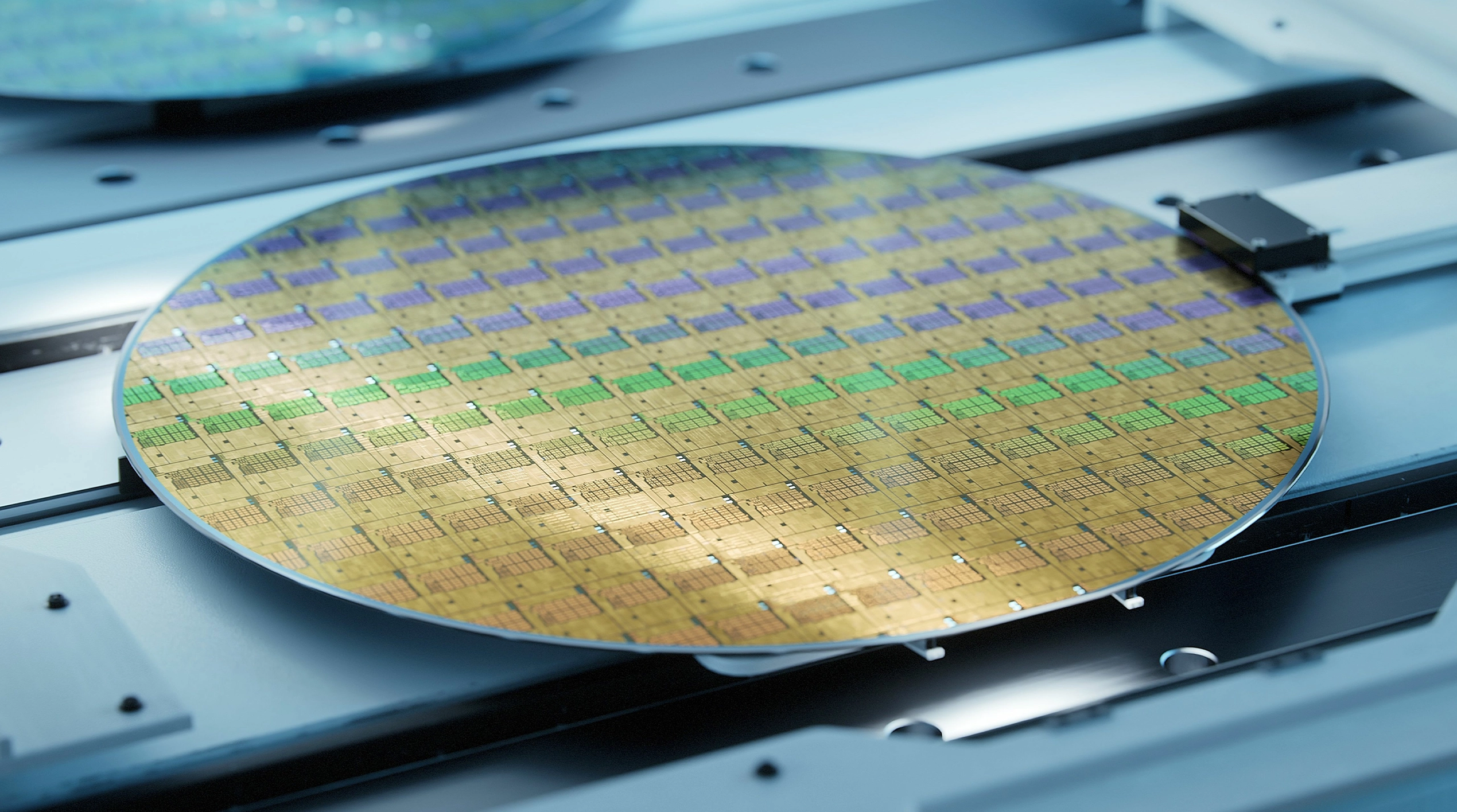
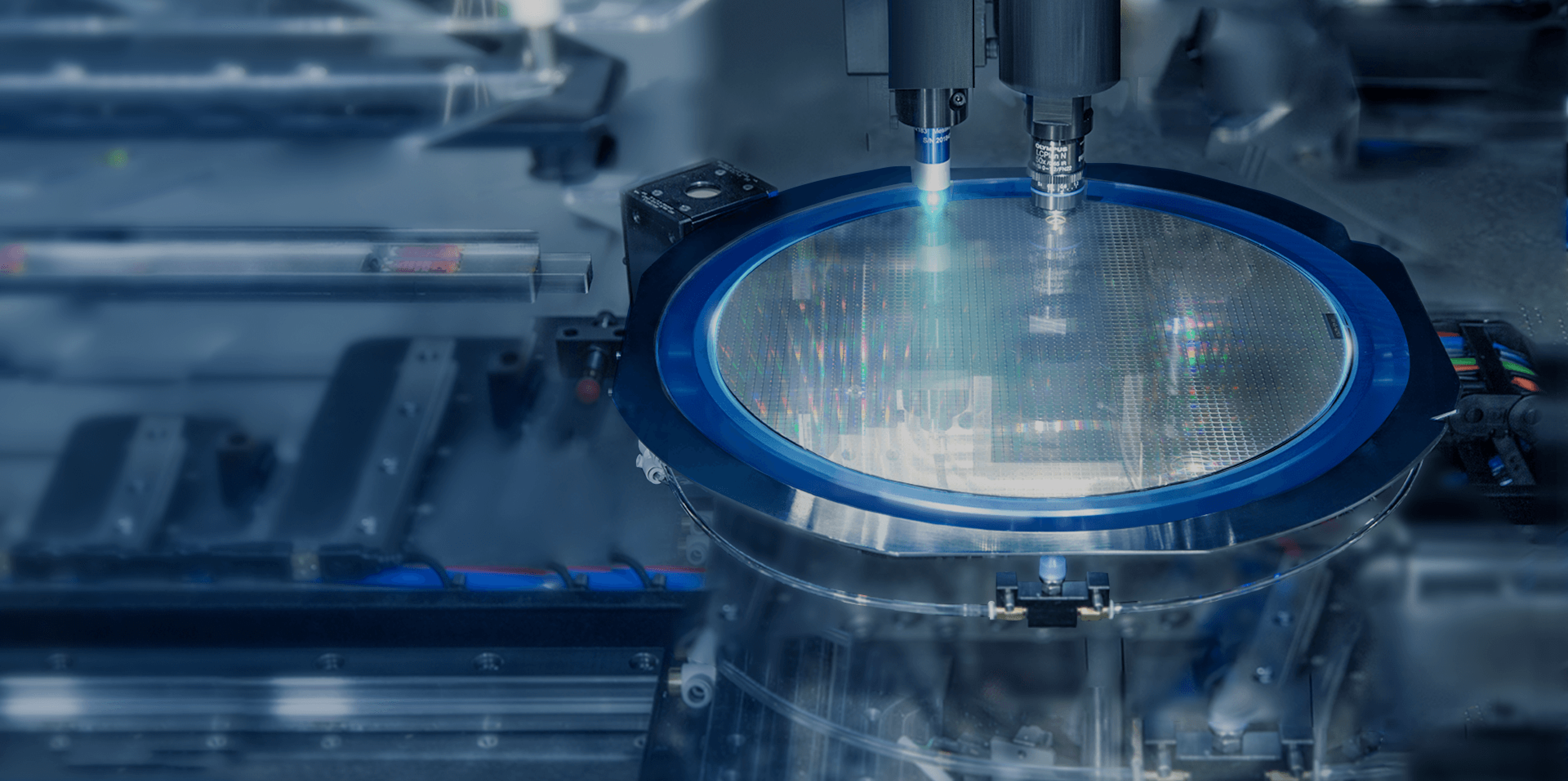
Laser stealth dicing has emerged as a premier non-contact singulation technology, bypassing the limitations of traditional mechanical sawing. By focusing a high-energy laser beam within the wafer's internal substrate, the process creates a localized modified layer without altering the top or bottom surfaces. Controlled external tensile or thermal stress is then applied to achieve precise, debris-free separation along the internal cleavage path. This non-contact mechanism completely eliminates edge chipping and micro-cracking, enabling ultra-precise micron-to-nanometer level dicing while drastically reducing cycle times and footprint overhead.

SFL-Quantum: Material-Specific Optimization & High-Yield Performance

SFL-Quantum’ wafer stealth dicing lasers are engineered to match the specific optical and physical properties of next-generation substrates, delivering exceptional edge quality and throughput across diverse material platforms:

Silicon (Si) Wafers: Achieves superior surface flatness and zero-debris kerfs, meeting the stringent topography requirements of high-density advanced packaging and IC manufacturing.

Silicon Carbide (SiC) & Gallium Nitride (GaN): Overcomes the extreme hardness and brittleness inherent to wide-bandgap (WBG) semiconductors. By precisely regulating internal stress distribution, the system minimizes micro-fractures, drastically reduces kerf loss, and maximizes die yield per wafer.

Wafer Processing
Semiconductor Inspection & Metrology

Semiconductor Inspection & Metrology

SFL-Quantum: Advanced Sub-Nanometer Interferometric Metrology Solutions

SFL-Quantum’s industrial laser systems combine ultra-narrow linewidths, high output power, and extended operational lifetimes to deliver industry-leading precision for in-line and offline wafer metrology. Leveraging high-coherence laser interferometry, these systems capture surface microtopography with sub-nanometer resolution, providing critical dimensional control over wafer thickness, global/local flatness, and shape distortion.

Silicon (Si) Metrology: Achieves thickness variation control within ±0.1um and scales flatness errors to the sub-nanometer regime—securing the stringent depth-of-focus (DoF) margins required for advanced lithography and etching.

Compound Semiconductors (GaN, SiC): Exceptional power stability enables deep penetration into multi-layer epitaxy. This allows for precise non-destructive measurement of epitaxial layer thickness and depth-resolved carrier/doping concentration profiles.

SFL-Quantum: Specialized OEM Customization & Process Integration

Recognizing that next-generation fabs require tailored inspection capabilities, Precilasers provides bespoke engineering services to match specific production line architecture:

Form Factor Flexibility: Seamless adaptation across standardized 8-inch (200 mm) and 12-inch (300 mm) wafer handling platforms.

Ultra-Wide-Band gap Substrates: Parameter optimization tailored to the unique refractive indices and physical properties of emerging materials like Gallium Oxide (Ga2O3) and Diamond wafers.

Automated Fab Integration: Turnkey optical sub-assembly optimization engineered to integrate directly with high-throughput automated material handling systems (AMHS).

Free space optical communication (FSOC)

Free Space Optical Communication (FSOC) utilizes light propagating in free space (air, outer space, or vacuum) to wirelessly transmit data at ultra-high speeds. By overcoming the bandwidth bottlenecks of traditional radio frequency (RF) technologies, FSOC serves as a cornerstone for next-generation, high-capacity communication networks across various demanding domains:

Last-Mile Connectivity & Mobile Backhaul: Enabling high-throughput, secure data backhaul between Low Earth Orbit (LEO) constellations, deep-space probes, and ground stations.

Disaster Recovery & Military Operations: Providing secure, jam-resistant, and license-free tactical communication networks in temporary or compromised environments.

Mitigating Atmospheric Turbulence: The Crucial Role of Sodium Guide Star Lasers

The primary bottleneck for high-speed terrestrial and satellite-to-ground FSOC is atmospheric turbulence, which causes wavefront distortion, beam wander, and severe signal fading (scintillation). To maintain stable, gigabit-to-terabit per second data rates, advanced ground stations integrate Adaptive Optics (AO) systems.

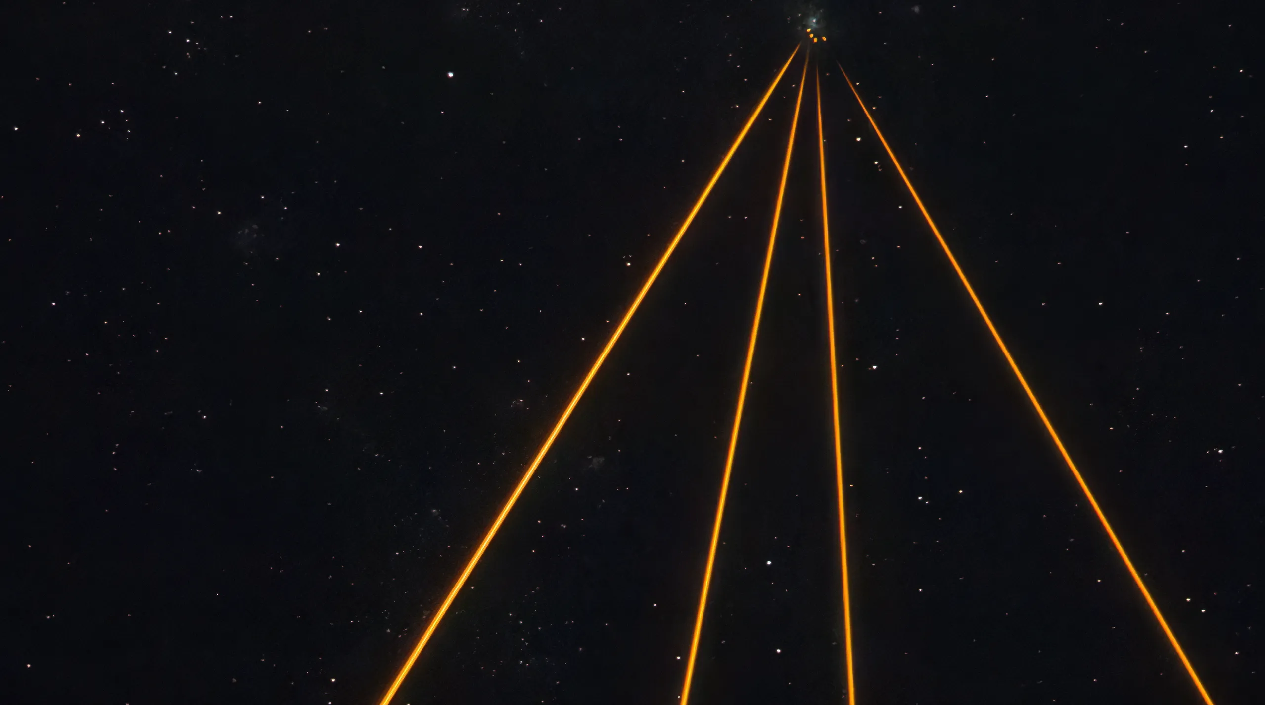
Artificial Beacon Generation: In scenarios where no bright natural stars are near the line of sight, a high-power Sodium Guide Star Laser (operating at the precise wavelength of 589nm) is projected into the mesosphere (at an altitude of approximately 90km).

Real-Time Wavefront Correction: This laser excites sodium atoms to create a bright, artificial "laser guide star." Ground-based wavefront sensors analyze the backscattered light to measure atmospheric distortion in real-time.

Optimized Signal Reception: Deformable mirrors in the AO system continuously correct the incoming signal beam based on these measurements, dynamically flattening the wavefront to dramatically improve coupling efficiency into the optical fibers of receiver systems.

Free space optical communication (FSOC)
Rydberg Atom Applications

Rydberg Atom Applications

SFL-Quantum: High-Power, Narrow-Linewidth Lasers for Rydberg Quantum Systems

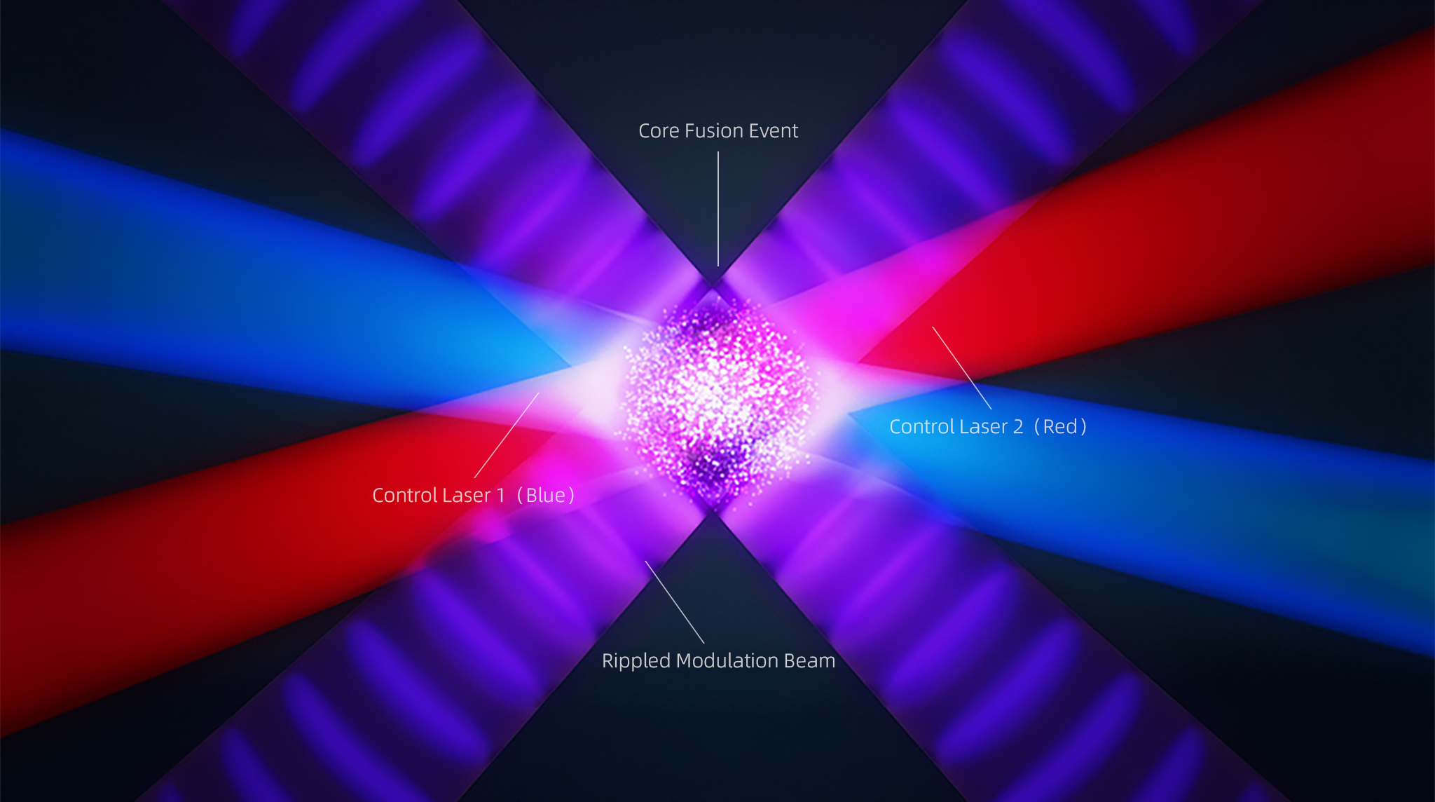
SFL-Quantum delivers a comprehensive portfolio of high-power, narrow-linewidth lasers spanning the UV to IR spectrum, specifically engineered for Rydberg atom excitation. Featuring exceptional spectral purity and frequency stability, these laser systems provide the precise optical coherence required for robust quantum state preparation and manipulation.

Core Applications

Quantum Precision Metrology: Enables ultra-high-sensitivity atomic electric field measurements (Rydberg EIT sensing) across RF and microwave bands.

Quantum Computing & Simulation: Delivers the high-power, low-phase-noise excitation necessary to drive scalable Rydberg atom logic gates and maintain long-lived quantum coherence.

Target-Specific Wavelength Coverage: Deeply engineered spectral matching for the critical cooling and repumping transitions of Strontium Monofluoride (SrF), Calcium Monofluoride (CaF), and Yttrium Oxide (YO).

CaF/SrF Cold Molecule Applications

SFL-Quantum: High-Power, Narrow-Linewidth Lasers for Ultracold Molecular Quantum Simulation

Ultracold molecules represent a frontier in quantum simulation, offering large electric dipole moments that enable long-range, highly tunable, and anisotropic dipole-dipole interactions compared to atomic systems. Realizing these advanced quantum architectures requires high-intensity, ultra-stable laser sources capable of driving robust laser cooling, magneto-optical trapping (MOT), and quantum state manipulation.

To meet these stringent demands, SFL-Quantum delivers a specialized portfolio of high-power, narrow-linewidth lasers optimized for mainstream molecular targets, including SrF, CaF, and YO.

Key Technical Specifications & Capabilities

Ultra-Narrow Linewidth: Less than 20KHZ short-term linewidth ensures exceptional phase coherence and precise addressing of narrow molecular transitions.

High Output Power: Up to 8W of continuous-wave (CW) output power, providing the high photon flux necessary for deep optical trapping depths and efficient spin-dependence tuning.

Target-Specific Wavelength Coverage: Deeply engineered spectral matching for the critical cooling and repumping transitions of Strontium Monofluoride (SrF), Calcium Monofluoride (CaF), and Yttrium Oxide (YO).

CaF/SrF Cold Molecule Applications